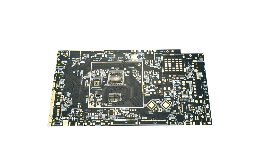
The ENIG Process Unveiled: A 9-Step Journey from Cleaning to Gold Plating
High-Reliability PCB The standard ENIG (Gold Plating) process consists of the following steps:
Degreasing → Micro-etching → Post-etch rinse → Pre-immersion → Activation → Post-activation rinse → Electroless Nickel Plating → Immersion Gold Plating → Rinsing
Why ENIG Dominates High-End PCB Finishes? 3 Core Advantages Explained
– Uniform Plating & Excellent Coplanarity
ENIG provides a flat, even surface with consistent nickel (3–5μm) and gold (0.05–0.15μm) layers, ensuring superior solderability, corrosion resistance, and wear resistance.
It is widely used in high-reliability electronics such as 5G modules, RF PCBs, and medical device control boards.
– Reliable Nickel Barrier Layer
The nickel layer acts as a barrier to prevent diffusion between copper and gold, ensuring robust solder joints for BGA and CSP assembly.
– Excellent Surface Protection
The immersion gold layer protects the nickel from oxidation, making it ideal for long-term storage and applications in automotive electronics (e.g., ADAS, BMS) and industrial automation PCBA.
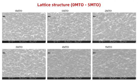
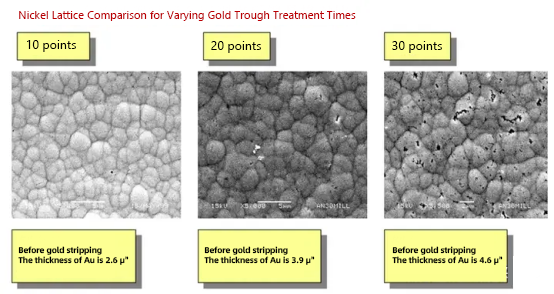
Chemical Precision: The Science Behind ENIG’s Tri-Layer Structure
(1) Activation
A thin, uniform layer of palladium (Pd) is deposited on the copper surface via displacement, providing catalytic activity to initiate the electroless nickel process.
(2) Electroless Nickel Plating
Under palladium catalysis, nickel ions are reduced by sodium hypophosphite, forming a Ni-P alloy layer (9–11% phosphorus), critical for high-density PCB layouts and multilayer PCB designs.
(3) Immersion Gold Plating
Gold is deposited via redox displacement, ensuring low signal loss for high-speed circuits and IoT control boards.
Layer-by-Layer Excellence: Functional Synergy in ENIG
– Palladium (Pd): Initiates electroless nickel deposition for high-precision soldering.
– Nickel (Ni): A Ni-P alloy base layer providing mechanical strength and thermal cycling resistance.
– Gold (Au): Oxidation-resistant surface for high-frequency PCB applications and smart sensor integration.
– Outstanding solderability for SMT assembly and fine-pitch components.
– Low failure rate PCBA with EMC/EMI compliance, ideal for telecommunication PCBs and wearable electronics.
– Zero defect PCBA assembly certified to RoHS, UL, and ISO 9001 standards.
– Controlled impedance design for 5G antennas and optical communication modules.
Surface Finish Showdown: ENIG vs Alternatives
| Finish Type | Advantages | Disadvantages | Best For |
|---|---|---|---|
| ENIG | Flat surface, oxidation resistance, fine-pitch & high-reliability | Higher cost (due to gold) | 汽车, medical, telecom, high-end electronics |
| HASL (Lead-Free) | Cost-effective, widely available | Uneven surface, poor for fine-pitch SMT | Low-end consumer electronics |
| OSP | Low cost, simple process | Short shelf life, humidity-sensitive | High-volume consumer boards |
| Immersion Silver/Tin | Good signal performance | Silver tarnish risk, tin whiskers | Mid-range digital & RF boards |
Recommended Applications of ENIG
– 📱 Smartphones, wearable device PCBA, tablet control boards.
– 🏭 Industrial sensor PCBA, automation control systems.
– 🚗 EV charging station PCB, BMS circuit design.
– 📡 IoT-enabled PCBA, Bluetooth module PCB, 5G infrastructure.
Why 500+ Global Enterprises Choose Our ENIG Solutions
✅ Turnkey PCBA Solutions
https://rmypcba.com/product-category/bare-pcb/
– Fast turnaround: 2–4 layer PCBs in 72 小时; high-mix low-volume support.
– Certified manufacturing: RoHS compliant, IPC-A-610 Class 3, ISO 13485 for medical devices.
✅ Custom ENIG Options
– Selective ENIG plating for cost-effective hybrid designs (e.g., gold fingers + OSP).
– High-speed PCB layout with controlled impedance for RF applications.
✅ Global Supply Chain
– 深圳Rimyi Technology Co., LTD with B2B wholesale capabilities and worldwide PCBA shipping.
https://www.youtube.com/@RIMYI
Get a Quote for Your ENIG PCB Today!
Need high-reliability PCBA for medical, automotive, or 5G applications?
Contact us for custom PCB design, rapid prototyping, and certified ENIG solutions tailored to your project!